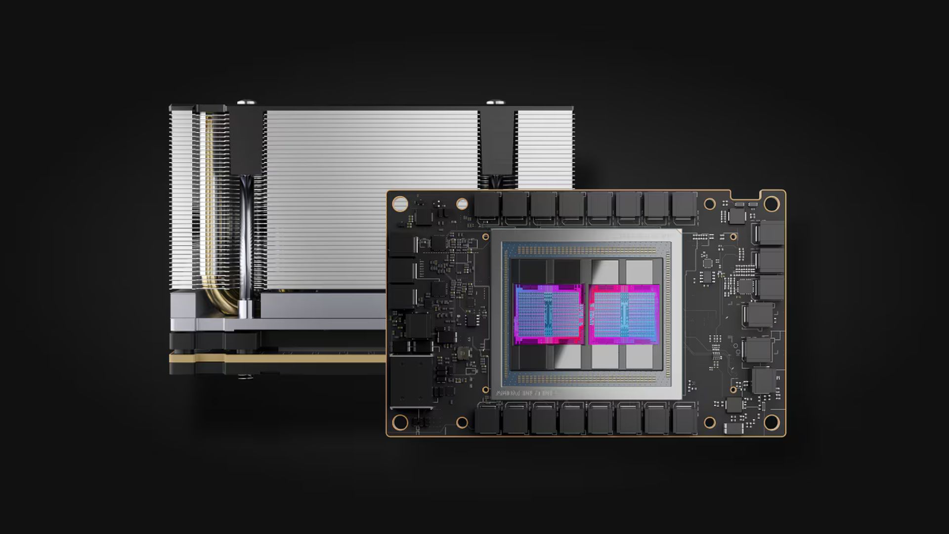
AMD announced its next-generation Instinct MI450 AI accelerators, based on the CDNA 5 architecture, will be manufactured using TSMC’s 2nm process technology. The AI accelerators are scheduled for introduction in the second half of next year.
The use of TSMC’s N2 fabrication process for the compute chiplets marks the first time AMD will employ a leading-edge manufacturing node for its AI GPUs. Lisa Su, chief executive of AMD, confirmed the technical details. “We are really excited about our MI450 generation, it has 2nm technology, so the most advanced fabrication capability, it has rack scale solutions, so we are really putting all of these compute elements together,” Su stated. “The way to think about it is it takes a village to build this all. So, you know, we are of course very, you know, proud and focused.”
This move represents a planned technological progression. AMD’s current-generation Instinct MI350-series accelerators, built on the CDNA 4 architecture, utilize compute chiplets produced on one of TSMC’s N3-series technologies, which entered mass production in late 2022. The transition to a 2nm-class process for the next-generation GPUs is a sequential step. The Instinct MI450 series will also be AMD’s first processors specifically tailored for artificial intelligence, incorporating support for dedicated AI data formats and instructions.
TSMC’s N2 node is designed to deliver “full node” improvements over its predecessors. The process offers a 10% to 15% performance increase at the same power and complexity, or a 25% to 30% reduction in power consumption at the same frequency. The N2 node also provides a 15% increase in transistor density compared to the N3E process. A key technological enabler is the use of gate-all-around (GAA) transistors, which allow developers to better tailor designs for maximum efficiency through design and technology co-optimization (DTCO). This migration to N2 provides AMD benefits across performance, efficiency, and density.
AMD’s manufacturing decision positions its product against upcoming hardware from competitor Nvidia. Nvidia has announced that its next-generation Rubin GPUs will be produced using one of TSMC’s N3 technologies, likely the N3P process tailored for its requirements. This places AMD’s Instinct MI450 on a more advanced manufacturing process compared to its rival’s announced plans.
A comparison of the companies’ planned rack-scale solutions reveals further differences. AMD’s Helios system, with 72 Instinct MI450 GPUs, will carry 51 TB of HBM4 memory and provide 1,400 TB/s of memory bandwidth. In contrast, Nvidia’s Rubin-based NVL144 machine will have 21 TB of memory and 936 TB/s of bandwidth. Nvidia’s system, however, is specified to offer higher FP4 performance, at 3,600 PFLOPS using its NVFP4 format, compared to the 1,440 PFLOPS for AMD’s Helios. The final performance and efficiency of the systems will also depend on factors like the UALink scale-up interconnections for the MI450-series GPUs.
OpenAI is reported to be one of the first customers to adopt the Instinct MI450, with hardware deliveries scheduled to begin in the second half of next year. Following this deployment, AMD anticipates a sharp revenue ramp-up. According to Su, the project will unfold over multiple phases and is projected to generate double-digit billions in incremental sales once fully operational. This alliance serves as a validation of AMD’s investment into its AI architectures and data center solutions.
Featured image credit


